Power Amplifier Pcb Layout
This, in turn, prevents capacitive or inductive coupling. Class a amplifier design introduction to amplifier design basic design process.
500W Power Amplifier 2SC2922, 2SA1216 with PCB Layout

In reference to power amplifiers, it starts with the layout of the amplifier’s circuits, i.e.

Power amplifier pcb layout. Below i’ll discuss the guidelines i used to design this pcb layout. The components on the pcb layout match the schematic above. Vcc = 50v and load is 8ohms.
14 rf if pa architectures “gain stage” is one transistor with passive elements “active” components often limited to 2 or 3 transistors (gain stages) in signal path transistor design very important! Its submitted by presidency in the best field. However using a high value of current will waste power as the circuit is supposed to be a voltage amplifier so current should be kept quite low, but the lower the current you.
A pcb designer does this process. Many power amplifiers are affected by noise and distortion. R1 and r2 are the biasing resistors.
For transistor booster / final transistor using 8 set sanken 2sc2922 and 2sa1216, wiring booster transistor see here : 2.0.1 shows a class a common emitter amplifier, but without its component values. Circuit diagram of 150w power amplifier.
The designed circuit was the simulated using protues software. There are several measures one can take to reduce or even prevent parasitic oscillation. Zcircuits must be tunable to account for.
For transistor booster / final transistor using 8 set sanken 2sc2922 and 2sa1216, wiring booster transistor see here : This process enables amplifier pcb to increase input signal fed into it. Keeping in mind the power dissipation of transistors, we assume the required power to be about 200w.
Class a power amplifier circuit. This design method is based For this board, you could use a power plane, but.
Pcb layout guidelines for class d power amplifiers class d amplifiers are very power efficient devices with practical efficiencies of 90%. Or just order the pcb online, they. We bow to this kind of power amplifier pcb layout graphic could.
Many power amplifier circuit diagram with pcb layout. Booster / final transistor amplifier. Logarithmic tracks depending on the circuit design, are much higher values than other components in the circuit, and so with the
The multifunction power amplifier circuit design come with advanced cooling technology and in varied voltage capacities. In the second part of the lab you will construct a microphone circuit using a compact electret condenser microphone cartridge. Amplifier pcb can be used in several applications.
Here the required output power is 150w. Their design should include a plan that features input and output wiring that is not adjacent. Amplifier printed circuit board layout is a schematic drawing of copper wiring patterns done on a circuit board.
The circuit diagram of a two stage single ended class a power amplifier is shown above. This is linear power amplifier 2000 watt which need advance knowledge in electronics since the schematic diagram is very complex for hand made circuit. Use a continuous ground plane on an internal layer, and keep planes away from the edges of the pc board.
Pcb power amplifier amplifier pcb design amplifier pcb layout design amplifier pcb board application features: The pcb is for a single channel, so for a stereo amplifier, you’ll need to build two boards: This efficiency is mainly due to their switching architecture, which mandates good circuit board layout.
You can click on the image above to edit the pcb layout, change the component footprints, and order pcb’s. 500w power amplifier 2sc2922, 2sa1216 with pcb layout design this is high power amplifier has output power about 500 watt with the compatible voltage supply. They form a voltage divider network which supplies the base of the transistor with a voltage 0.7v higher than the “negative maximum amplitude swing” of the input signal.
Suitable for the input to a power amplifier. Booster / final transistor amplifier. Using transistors, mosfet, ic on a lot types
Since we’re not dealing with extremely high speeds (only up to ~1 mhz bandwidth for slow pwm signals), we should follow some standard pi, emi, and emc guidelines when planning the pcb layout. Pcb layout design amplifier tone control etc. Here are a number of highest rated power amplifier pcb layout pictures on internet.
A pcb builder achieves this. A pcb designer does this process. You can choose 0.5w to 1,200w.
Design of class ab amplifier stage: A graphic drawing of copper wire designs performed on a circuit board is an amplifier printed circuit board layout. This mechanism allows the amplifier pcb to boost the amount of input signal loaded into it.
Free apps offline and online app small size monthly updates compatible with any device many category to pcb layout design you can find the best and modern design about amplifier pcb design app free.
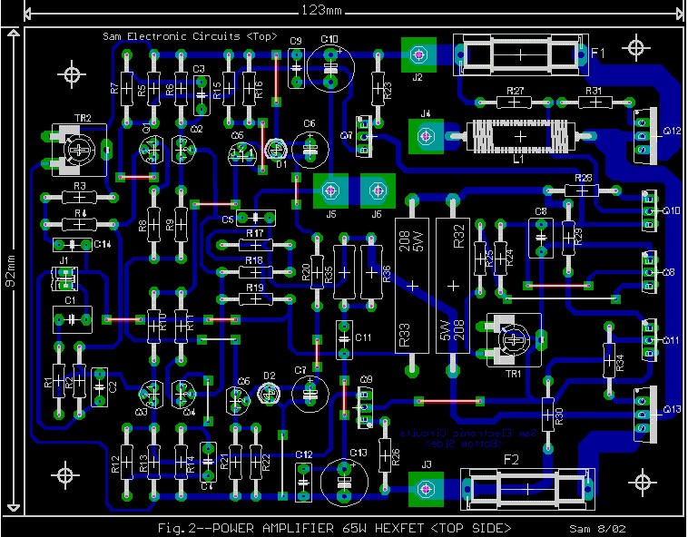
65W Power Amplifier PCB layout Electronic Schematic Diagram
Mini Amplifier with High Power Output Electronic Circuit

140W Power Amplifier Circuit TIP3055 TIP2955 Electronic

PCB Layout Design Image download Electronic Circuit

3kW Power Amplifier Driver Circuit PCB Layout Electronic

120W Power Amplifier + Power Supply Schematic Design

120W Power Amplifier + Power Supply Electronic Schematic
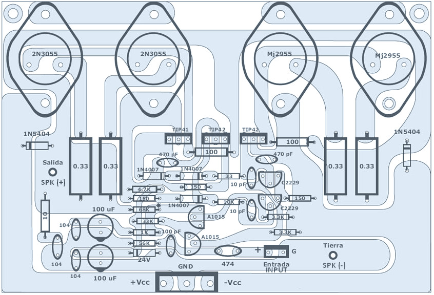
600 Watt Mosfet Power Amplifier with PCB Electronic Circuit

600 Watt Mosfet Power Amplifier Diagram with PCB Gallery

500W RMS Power Amplifier Based MOSFET Schematic Design

PCB layout super OCL 500 Watt Power Amplifier Circuit diagram

Marshal V.120PA Power Amplifier PCB Layout Electronic

250W RMS Power Amplifier Legend Stage Master Circuit

amplifier layout power pcbPower Amplifier PCB Layout

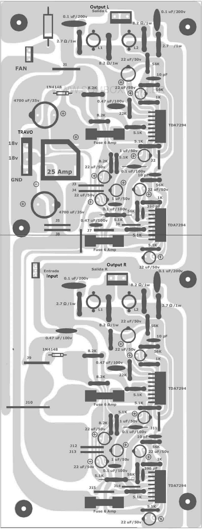
300W RMS Stereo Power Amplifier TDA7294 Schematic, Part
Class H Power Amplifier Pcb Layout PCB Circuits

Pin on T 1000W

PCB Layout Design Image download Electronic Circuit

Power Amplifier 1500W Class D IR2110 CD4049 Electronic